EncoderCAT PCB
The PCB has the following fetaures:
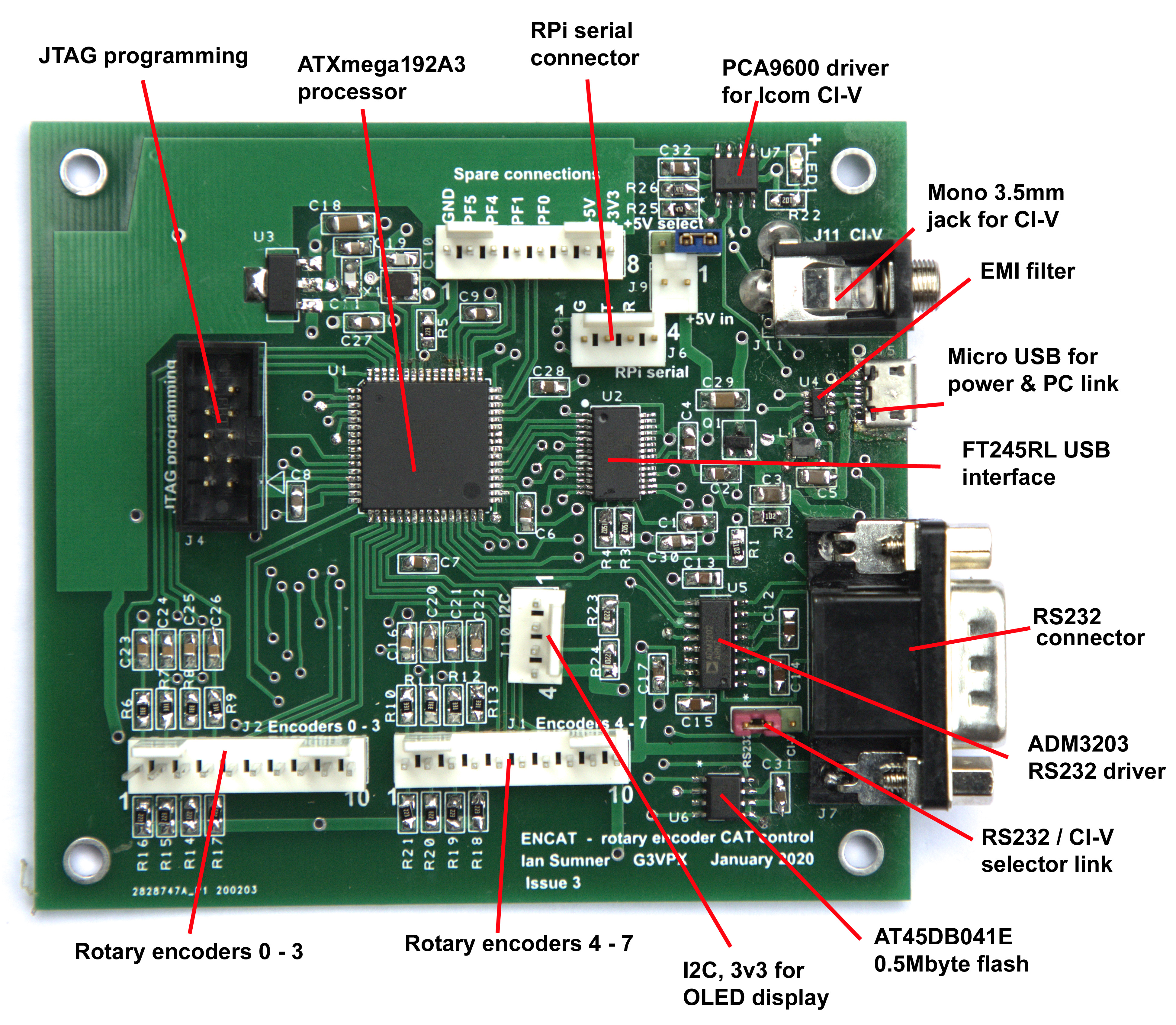
- PCB size is 8.5 x 9.5 cm. (My discarded issue 1 and 2 PCBs make good beer mats!)
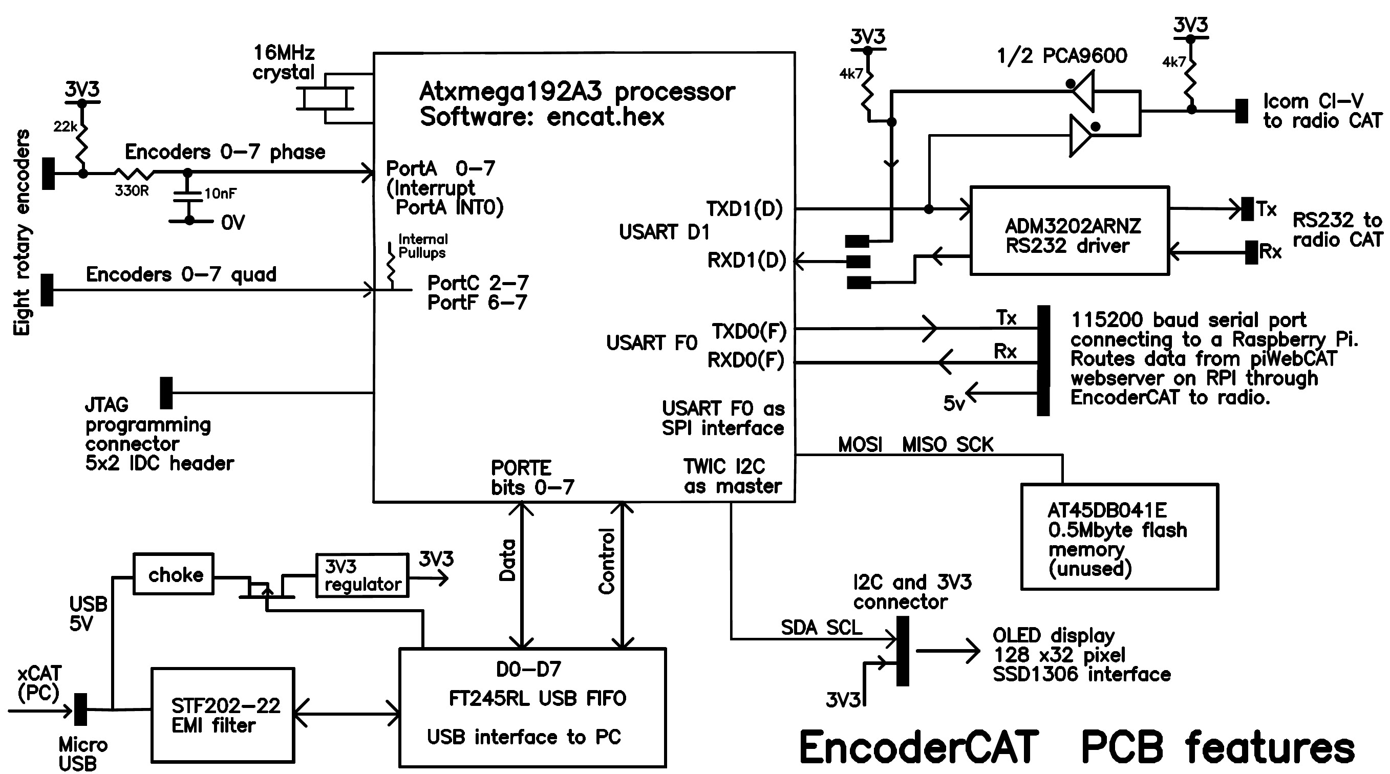
- Atmel Atxmega192A3 processor running at 32MHz. (16MHz crystal + PLL doubler enabled)
- RS232 (+5v / -5v) CAT interface drive using an ADM3203 device.
- Icom CI-V CAT interface - single wire bidirectional, wire-ored. Driven by a NXP PCA9600 device.
- Input connectors for eight rotary encoders (low resolution .. eg: car radio volume controllers)
- Power supply - 5v - via micro USB or dedicated power connector.
- Configuration via USB using xCAT PC application. (FTDI FT245RL device)
- Configuration stored in processor's 2kbyte EEPROM memory.
- 115200 baud serial connector to a Raspberry Pi for integration with piWebCAT.
- I2C connector (with 3v3 power) - used for 128x32 OLED display.
- Adesto AT45DB041 0.5 Mbyte flash memory device for future expansion or alternative PCB usage,
- JTAG programming connector.
- The PCB could be used for other projects - eg: controlling a home brew transceiver.
- It has USB, fast serial, RS232 and I2C connectors plus sixteen bit digital I/O.
- It has a 0.5Mbyte flash chip - which is unused in EncoderCAT.
- The number of digital I/O lines could be increased using the I2C interface
eg: using a PCA9555 I2C to 16 line decoder,
see http://www.homebrew-radios.net/trxavr_picastar/I2C/PCA9555_board.htm
The PCB schematic is available as a downloadable PDF at: http://encat.g3vpx.net/files/encat-schematic.pdf
Note that the AT45DB041E device is not used and so can be omitted ( They cost £1.05 + VAT from Farnell !).
The PCB shown above was designed using Easy-PC software and commercially manufactured.
Using Easy-PC:
Every component has a schematic symbol and PCB footprint (copper, drilling, top silk etc).
A component record then combines the schematic and PCB records and maps the pin numbering between them.
The schematic diagram is built using the schematic symbols.
'Forward design changes' then transfers the schematic design to the PCB layout
placing all components in a 'component bin'.
Then, as components are dragged from bin to layout, connections are shown as straight, fine dotted lines.
These are then manually replaced by PCB tracks.
The software prevents the operator from making connections which are illegal according the schematic.
A final integrity check warns of any electrical discrepancies between layout and schematic.
At the time of writing, G3VPX had 50 bare PCBs available for sale at low cost.
.. more can be manufactured at 2-3 weeks notice.
Home fabrication would be possible using double sided construction with wired-through vias.
This would however require a totally new layout, mainly because of the wired vias:
- Wired vias cannot be located underneath surface mounted ICs.
- Wired vias on home brew boards need to be larger to cope with alignment inaccuracies
between the two sides of the board.